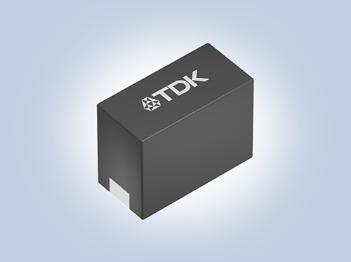
•This component achieves a high inductance of 10 μ H in a small package size of 1206
• High impedance characteristics within a wide frequency range of 10MHz to 200MHz
•The DC resistance is reduced by about 70%, and the rated current is increased by 1.7 times

The actual appearance of the product is different from the picture.
The TDK logo is not printed on the actual product.
TDK Corporation (TSE: 6762) has expanded its PLEC69B series (length x width x height: 1.2 x 0.6 x 0.95mm) thin film inductor products. This series of products is used in artificial intelligence (AI) data center optical transceivers to separate data signals from power. The new product has started mass production in August 2025.
With the widespread application of artificial intelligence, the demand for high-speed and high-capacity optical transceivers is rapidly increasing. The bias T-shaped circuit used in these transceivers can superimpose signals and power on the same transmission line. Inductors such as PLEC69B can utilize impedance characteristics to separate signals from the power supply in biased T-shaped circuits, preventing signals from flowing into the power supply side.
The new product adopts TDK's proprietary metal magnetic materials and structural design, achieving the highest standard performance of 10 μ H inductance at 1206 size *. In the wide frequency range of 10MHz to 200MHz, signals can be separated from the power supply by high impedance, thereby improving communication quality. In addition, the DC resistance is 1.4 Ω (typical value), which is about 70% lower than similar products on the market. This can reduce power loss and heat generation. The rated current (Isat) is 0.2A, which is 1.7 times higher than similar products. In addition, the smaller size also saves PCB space. The maximum operating temperature of PLEC69B can reach+125 ° C, ensuring high reliability.
TDK will continue to develop low-power and high-speed communication products, enrich its product lineup, and meet market demand. These products are designed specifically for data centers, servers, optical communication equipment, and edge devices, providing support for the significantly growing artificial intelligence market in the future.
*Source: TDK, as of August 2025
Term
Biased T-type circuit: a circuit that can superimpose and separate signals and power sources on a single transmission line
Main applications
• Used for signal circuits: bias T-shaped circuits in optical communication modules
• Used for power circuits: smartphones, true wireless stereo (TWS), wearable devices
Main features and advantages
• Has high impedance characteristics, with a frequency range of 10MHz to 200MHz
The DC resistance is reduced by about 70%, with a typical resistance value of 1.4 Ω, which helps to reduce power loss and heat generation
Rated current (Isat) is 0.2A, increased by 1.7 times


