Infineon launches CoolSiC packaged in Q-DPAK ™ MOSFET 1200 V G2, Raise the power density of industrial applications to new heights
On August 1, 2025, Munich, Germany, Infineon Technologies, a global semiconductor leader in power systems and the Internet of Things, recently launched CoolSiC with top cooling (TSC) Q-DPAK packaging ™ MOSFET 1200 V G2。 This new type of semiconductor device can provide better thermal performance, system efficiency, and power density, designed specifically to meet the high-performance and high reliability requirements of industrial applications, such as electric vehicle chargers, photovoltaic inverters, uninterruptible power supplies, motor drives, and solid-state circuit breakers.
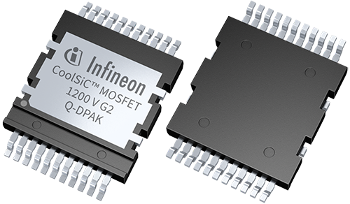
CoolSiC packaged in Q-DPAK ™ MOSFET 1200 V G2
The technology used in this CoolSiC 1200 V G2 has significantly improved compared to the previous generation, reducing switch losses by up to 25% and increasing system efficiency by 0.1% while maintaining the same on resistance (Rds (on)). Based on Infineon's advanced technology XT diffusion welding technology, , The thermal resistance of G2 series products is reduced by more than 15% compared to G1 series, and the MOSFET temperature is also reduced by 11%. With excellent on resistance ranging from 4 m Ω to 78 m Ω and a rich product portfolio, designers can flexibly use it to improve system performance and meet target application requirements. In addition, the new technology supports overload operation at junction temperatures up to 200 ° C (Tvj) and has excellent anti parasitic conductivity, ensuring reliable operation under dynamic and harsh conditions.
Infineon CoolSiC MOSFET 1200 V G2 is available in both single switch and double half bridge Q-DPAK packages. Both models belong to Infineon's broader X-DPAK top cooling platform. The packaging thickness of all top heat dissipation (TSC) versions (including Q-DPAK and TOLT) is uniformly 2.3 mm, providing high design flexibility, allowing customers to flexibly expand and combine different products under a single heat sink component. This design flexibility simplifies the development of advanced power systems, making it easier for customers to customize and expand their solutions according to their needs.
The Q-DPAK package significantly improves heat dissipation performance by achieving direct thermal conduction between the top of the device and the heat sink. Compared with traditional bottom heat dissipation packaging, this direct heat conduction path can significantly improve the heat conduction efficiency and make the system design more compact. In addition, the layout design of the Q-DPAK package significantly reduces parasitic inductance, which is crucial for improving switching speed, enhancing system efficiency, and reducing the risk of voltage overshoot. Due to its small footprint, this package is suitable for compact system designs, and its compatibility with automated assembly processes simplifies the manufacturing process, ensuring cost-effectiveness and scalability.
Supply situation
CoolSiC with Q-DPAK single switch and dual half bridge packaging ™ MOSFET 1200 V G2 is now available on the market.